The future of lithography
Can top-down nanotechnology keep getting better?
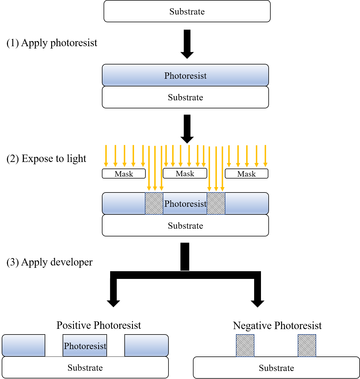
Photolithography works by shining light over a patterned “mask” and on to a silicon wafer coated in “photoresist”. Where the light hits the resist, the resist can be removed, leaving behind a pattern that matches the mask. From there, additional tricks turn these patterns into actual, wired-together transistors. This process is central to semiconductor manufacturing.
It’s a truly incredible technique that can fabricate arbitrary patterns at a resolution of a few tens of nanometers. Considering that atomic bonds are roughly 0.1 nm at their smallest, we’re tantalizingly close to atomic precision.
But current photolithography techniques are nearing their limits and the industry is scrambling to find new solutions. What’s next for semiconductor manufacturing? Will we ever reach the atomic scale?
Pushing the limits with X-rays and Electrons
The most straightforward way to increase resolution of a photolithography technique is to increase the frequency of the light. Fabs have lowered the wavelength of the light source in distinct stages over the last few decades, with each stage requiring significant changes to the production process. Our most advanced light source, extreme UV, produces 13.5 nm light through extraordinary feats of engineering.
(I highly recommend watching this video to get a sense of the scale of research effort that goes into semiconductor manufacturing. The entire video is devoted just to the light source; every step of semiconductor manufacturing requires a similar attention to detail.)
So the clear next step would be to generate higher frequency, higher intensity light using something like a free electron laser or synchrotron. Unfortunately, this equipment is extremely expensive and the secondary electrons generated by high energy light already limit resolution in EUV. More powerful light sources might only make things worse.
Another possibility is electron beam lithography. These systems actually have a higher resolution than current photolithography techniques (under 10nm!), but the throughput is so low that the chips are prohibitively expensive. Could rising demand for compute eventually make these chips viable? I doubt it, at least in the short-term1, the semiconductor industry actually seriously considered electron beams before choosing EUV. However, electron beams are still useful for creating masks and metamaterials, which we’ll explore in the next section.
Superresolution
There are a few clever tricks the industry has used to squeeze more resolution out of a lithography system. The first is multi-patterning, where you lay down two separate patterns that are a half shift apart, effectively doubling the resolution.
The second trick is to design photomasks that take into account the strange dynamics of light. Using computational lithography, masks can take advantage of interference patterns to improve the precision of the resulting design. In the limit, these masks become metalenses, or nanostructures that reshape light to achieve superresolution lithography. It may be possible to go even further by leveraging the quantum properties of light or electrons2.

I can’t help but note parallels to X-ray diffraction techniques and electron diffraction, where the atoms of a crystal act as a diffraction grating. Could the diffracted patterns from these techniques be leveraged for lithography?
Other tricks
Here, I’m going to entertain some far-out speculation on how fabs could push for even higher resolutions.
Diamond immersion lithography: Today’s lithography techniques pass light through ultrapure water because the higher index of refraction produces smaller features. Diamond has an even higher index of refraction, so perhaps a block of diamond grown with chemical vapor deposition could lower feature size.
Laser coupled particle beams: Combining different beams (or multiple beams) can lead to new effects. Cold, laser coupled particle beams have miniscule divergence, could these be used to punch tiny holes in a thin membrane and produce a photomask?
Iterated implosion fabrication and nanoimprint lithography: Implosion fabrication shrinks a pattern embedded in a shrinkable polymer. Nanoimprint lithography works by stamping a surface with a nanoscale pattern. Could we stamp a hydrogel and then shrink it to obtain a finer resolution? What stops us from repeating this process by using the smaller pattern to stamp a fresh surface and shrink further?
Metalenses that make metalenses: Intricate metalenses can act as masks that produce a desired pattern. What if we used a metalens to create an even more intricate metalens? What is the limit of iterating this process?
Self-assembling molecules: Molecules can self-assemble into interesting patterns (e.g. MOF’s, COF’s, SAM’s, block copolymers, etc), these self-assembled patterns could act as photomasks, shaping light or electrons into a desired pattern. Peptides could be used to precisely place atoms.
DNA origami masks: DNA can designed to fold into intricate 2D patterns which may be useful as a photomask.
Atomically precise placement: Techniques like atomic force microscopy can place atoms and molecules at precise locations. This could be used to fill in spaces on a photomask at a finer resolution than is feasible with electron beams.
Trapped ions and cold atoms: Ion traps and optical tweezers can arrange atoms into various patterns and manipulate their quantum states. These arrays of atoms could be used to manipulate beams of light or electrons.
Plasma wakefield acceleration for high quality electron beams
Conclusion
Computers aren’t the only product that stands to benefit from top-down nanotechnology. The enchippening will come for fields like chemistry, spectroscopy, communications, medicine, materials science3, and energy production.
Despite the heralded end of Moore’s law, innovation in lithography techniques will continue for a long time4. As transistor density has plateaued, the industry has started to fab transistors on top of each other, stitch chiplets together, and use wafer-to-wafer stacking to increase performance5. The co-design of algorithms with hardware will squeeze more performance out of each transistor while compute marketplaces will ensure that existing chips are fully utilized.
Let’s hope that one of the greatest engines of progress in the 21st century can continue into the 22nd.
(EDIT May 11th: I added more explanation of what photolithography is)
In the long-term electron beams are very interesting if people can make e-beam equipment cheap and write with multiple beams on a single instrument. Atomic Semi is doing interesting work making e-beam fab cheaper.
One bizarre trick is to use interaction-free or gentle measurement of a system to make electron beams less destructive.
One thing I didn’t get a chance to talk about is how atomic layer deposition and atomic layer etch can add or subtract atomic layers of a variety of different materials. Getting these techniques to encompass a wider range of materials and smaller spatial patterns will let us build unprecedented condensed matter systems.
Unconventional computing paradigms will piggyback off of this progress, leading to continued performance gains.
What’s stopping us from building solid blocks of compute complete with their own (microfluidic, thermoelectric, solid-state fan, etc) cooling systems, photonics, and antennas? Macroscale, self-sufficient computing machines sound similar to computronium.


Great explainer here Sam. I don't know how you keep up with all of these tech pathways. A decade or so ago, I lamented the end of Moore’s Law and the fact that we were approaching the limits of how small we could produce transistors.
Today I celebrate the power of innovation and how, despite the challenges, we have continued to see improvements in computing capability despite growing physical limitations.
Innovation is hard.
It would be easier to read if there was a more detailed explanation of the concept of photolithography itself.